Prior Scientific - H112
Manufactured by Prior Scientific
No Documents
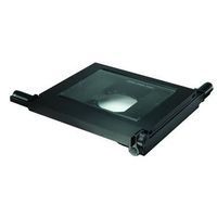
The H112 stage is ideal for scanning a wide range of semiconductor wafers, photo masks, flat panel displays and printed...
The H112 stage is ideal for scanning a wide range of semiconductor wafers, photo masks, flat panel displays and printed circuit boards. The H112 can easily accommodate 12 inch (300 mm) wafers and works with many robot arm wafer loaders. In addition, the H112 can be used for transmitted light applications with 250 mm x 250 mm transmitted light area.
Active Questions & AnswersAsk a Question
There are no current Discussions
Microscope Accessories Service ProvidersView All (10)
Documents & Manuals
There are no Documents or Manuals available.
Features of H112
- Suitable for most major brand microscopes. * 1µm or better repeatability * Optional 100nm linear scales provide the highest resolution available. * Wide range of wafer holders * 300 mm x 300 mm (12"x12") travel
General Specifications
There are no General Specifications available.