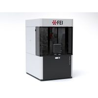
FEI Company - Helios G4 FX DualBeam™
Manufactured by FEI Company
No Documents
Enabling development of 7nm devices with shorter time to data
Enabling development of 7nm devices with shorter time to data
The FEI Helios G4 FX DualBeam™ miceoscope is FEI's most advanced failure analysis DualBeam platform, capable of creating high-quality, ultra-thin TEM lamellae for 7nm process development and ramp. Containing the all-new, high-performance Phoenix focused ion beam (FIB) column, the Helios G4 FX DualBeam allows operators to quickly and efficiently create ultra-thin lamellae with minimal damage and maximum cut fidelity. Combining the highest-resolution Elstar+UC scanning electron microscope (SEM) column and the FEI EasyLift Nanomanipulator, the Helios G4 FX DualBeam makes endpointing and in-situ sample lift-out easier than ever. FEI's unique MultiChem Gas Delivery System provides optimized beam-assisted deposition and etching capabilities. In addition to simplifying the process for advanced failure analysis and TEM sample preparation, EasyLift and MultiChem improve operator confidence and consistency, reducing overall system Cost of Ownership. The Helios G4 FX DualBeam is also the first DualBeam system to include sub 3Å-resolution STEM imaging, providing advanced Pathfinding Labs with much shorter turnaround times to high quality data. The ability to quickly produce high-quality, actionable 30kV STEM images within the DualBeam provides a clear advantage to FA labs and process developers.
The world's most advanced DualBeam platform for imaging, analysis, and TEM sample preparation in semiconductor pathfinding and process development laboratories.
The FEI Helios G4 FX DualBeam combines the industry-leading, highest-resolution Elstar+UC SEM with the most advanced Phoenix FIB for best-in-class imaging and milling performance. Added to this field-proven, fourth-generation Helios platform are the most advanced in situ lift-out and sample manipulation components, an innovative multiple gas delivery system, a dramatically improved 3Å-resolution, low-kV STEM detector, and customizable recipes, creating the most capable and flexible failure analysis instrument available today.
Cross Section Imaging
The innovative Elstar electron column with UC monochromator technology provides the foundation of the systems' unprecedented high-resolution imaging capability. This translates to uncompromised SEM resolution of 0.6nm at optimum working distance and 0.8nm at dual beam coincidence. High-resolution, low-damage electron beam imaging is critical for identifying defects or structural problems within the bulk sample and endpointing on ultra-thin TEM lamellas. Operating at very low landing energies is also critical to minimize beam-induced damage on sensitive materials such as low-k dielectric or photoresist.
Shorten time to data
The Helios G4 FX DualBeam comes with a new compustage for TEM grid handling and G4 STEM detector to support inverted lamella preparation, a critical workflow for creating high-quality, ultra-thin samples for STEM or TEM, and provides new capability to shorten the time to useable data. The dedicated compustage and double-tilt STEM rod holder provide five axes of rotation to facilitate SEM endpointing on both sides of the lamella, and allows the operator to easily create inverted or plan view samples. As lamella thicknesses continue to shrink, the higher energy electrons in standalone S/TEM systems (generally operating at >80 or 120kV) have very little material to interact with in the sample. Thinner and thinner lamellae require lower and lower electron beam accelerating voltages to allow electrons more interactions with different materials in the sample, a necessary step for maximizing materials contrast and delineating interfaces. The all-new G4 STEM detector, in combination with a 30kV electron beam, has been shown to have improved sensitivity to materials with similar atomic mass than previous STEM detectors in DualBeam systems. The ability to complete failure analysis work in the DualBeam with a low-kV STEM image-without exposing the finished sample to ambient air-shortens the time to data and reduces the need for standalone S/TEM systems.
Active Questions & AnswersAsk a Question
There are no current Discussions
Electron Microscopes Service ProvidersView All (8)
Documents & Manuals
There are no Documents or Manuals available.
Features
There are no Features available.
General Specifications
There are no General Specifications available.