Bruker Optics - JV Sensus
No Documents
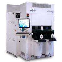
X-Ray Diffraction Imaging (XRDI) inspection>The JVSensus is the latest defect metrology system...
The JVSensus is the latest defect metrology system for Si device manufacturers. It helps identify problems encountered during wafer production using the latest X-ray diffraction imaging (XRDI) technology. Applications include monitoring edge damage to prevent costly wafer breakage during ultra fast anneal. It can qualify and monitor process tools at any technology node, which reduces cycle times and facilitates fab expansion.
Active Questions & AnswersAsk a Question
There are no current Discussions
X-ray Diffraction Service ProvidersView All (9)
Documents & Manuals
There are no Documents or Manuals available.
Features of JV Sensus
Easily Identify Crystalline Defects JVSensus enables its users to identify cracks and other defects in the wafer which can cause catastrophic structural failure, BEFORE the breakage occurs. Once a defect has been observed, non-destructive cross section review images can be performed to locate the defect locations within the wafer depth.
Measure on Patterned Wafers Measurements can be performed on blanket, patterned, and metalized wafers without sample preparation. The defects can be identified even when a pattern is present on the wafer. Robot loading can be added for wafers sizes from 2” to full 300mm
Detect Slip The major cause of overlay issues is slip. Whether it's a logic patterned wafer, GaN on Si or ingot slides , JVSensus can detect slip in minutes.
General Specifications
There are no General Specifications available.