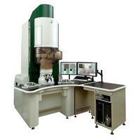
JEOL - JEM-ARM200F
No Documents
Highest Resolution Analytical S/TEM in Its Class
Active Questions & AnswersAsk a Question
Recent Questions & Answers
Electron Microscopes Service ProvidersView All (8)
Documents & Manuals
There are no Documents or Manuals available.
Features of JEM-ARM200F
Environmental measures The JEM-ARM200F offers the ultimate stability for imaging and analysis at the atomic scale. The electron column is isolated from the environmental disturbances found in most labs. A superior shielding design safeguards the ultrahigh-powered optics from airflow, vibration, acoustical, and electronic interference, magnetic fields, and thermal fluctuations.
Enhanced mechanical stability To enable atomic level analysis and imaging - utilizing spherical aberration correctors for electron optic and image forming systems - vibration and distortion on the atomic level need to be controlled. The ARM 200F features an overall mechanical strength twice higher than conventional TEMs. Enlarging the column size improves rigidity and optimizing the console structure enhances mechanical stability.
Enhanced electrical stability The ARM200F reduces the fluctuation of the high voltage system and the objective lens current by 50% of that of conventional TEMs, significantly enhancing its electrical stability.
Wide ranging STEM analytical capabilities Two types of dark field detectors with different STEM detection angles (one as standard), a bright field detector (standard), and a backscattered electron detector (option) can be simultaneously installed. A new scanning image acquisition system is capable of acquiring 4 different types of signals, enabling simultaneous observation of all 4 images.
Optional spherical aberration corrector for TEM image forming system With an optional spherical aberration corrector, the resolution of the TEM image can be improved to 0.11 nm.
Integrated Software Automation The latest in software automation has been designed into the new ARM200F, with tomography and holography simplified by a user-friendly GUI.
General Specifications
| Magnification | 200 to 150000000 x |
| Accelerating voltage | 80 to 200 kV |
| Electron Microscope Type | TEM |
| Microscope Type | Electron |
Additional Specifications
Resolution
Scanning transmission image: 0.08 nm (at 200kV)
Transmission image: 0.19 nm (at 200kV)
Point image: 0.11 nm with TEM Cs corrector 3) (at 200kV)
Lattice image: 0.10 nm
Magnification
Transmission image: 50 to 2,000,000x
Electron gun: Schottky field emission gun
Specimen Stage
Stage: Eucentric side entry goniometer stage
Specimen size: 3 mm dia.
Tilt angle: Up to 25° (with double tilt holder)
Movement range: X/Y: ±1.0 mm (motor drive/piezo drive)
Cs Correctors
STEM Cs corrector: Standard
TEM Cs corrector: Optional
Optional accessories: Energy Dispersive X-Ray Spectrometer (EDS)
Electron energy-loss spectrometer (EELS)
CCD camera, etc.