JEOL - JEM-3100F
Manufactured by JEOL
No Documents
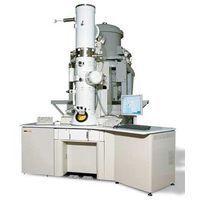
JEM-3100F Transmission Electron Microscope
The JEM-3100F field emission transmission electron microscope has a resolution of 0.17 nm, the best available for this class of microscope. The high resolution of the JEM-3100F is especially effective in the testing of nano technology materials. The control system uses state-of-the-art digital technology, and substantially enhances ease of operation.
With an accelerating voltage of 300 kV, the JEM-3100F is suitable for process testing, and is capable of inspecting relatively thick semiconductor devices sectioned by a focused ion beam at high throughput.
The JEM-3100F is an indispensable tool in a wide range of applications from research and development to manufacturing; including biology, basic materials research and development, failure analysis, and quality control.
Active Questions & AnswersAsk a Question
There are no current Discussions
Electron Microscopes Service ProvidersView All (8)
Documents & Manuals
There are no Documents or Manuals available.
Features of JEM-3100F
- Resolution of 0.17 nm, the best available for this class of microscope
- High brightness, high stability Schottky electron gun ideal for analysis
- New 5 axis motor drive goniometer for enhanced stage accuracy
- Fully digitized control for ease of operation
- Upgraded to support micro area elemental analysis when JEOL’s scanning transmission electron microscope (STEM) system and an energy dispersive X-ray analyzer (EDS) are incorporated
General Specifications
| Magnification | 60 to 1500000 x |
| Electron Microscope Type | TEM |
| Probe Current | 0.5 nA or higher/1nm |
| Microscope Type | Electron |
Additional Specifications
TEM particle resolution: UHR 0.17 nm (UHR)
STEM resolution: 0.14 nm (UHR/HR)
(Optional STEM and dark field imaging device needed)
Information limit: <0.1nm
Accelerating voltage: 300 kV (200 kV and 100 kV optional)
Electron gun:ZrO/W (100) Schottky
Brightness: 7x10⁸A/cm2sr or higher
Convergent angle: 1.5 – 20 mrad or higher (UHR/HR)
Specimen movement: XY: 2 mm; Z: 0.2 mm (UHR)
EDS (Optional): Solid angle 0.13 sr (UHR/HR)